What is PCB Make? A Complete Guide to Designing and Manufacturing PCBs
The world of electronics is rapidly evolving, and at the heart of this transformation lies an essential component: the printed circuit board (PCB). As the backbone of virtually all electronic devices, understanding "pcb make" processes is crucial for engineers, designers, and manufacturers alike. According to a report by MarketsandMarkets, the global PCB market is projected to reach USD 93.76 billion by 2025, growing at a compound annual growth rate (CAGR) of 4.2%. This growth signifies an increasing demand for advanced PCBs, driven by sectors such as automotive, industrial, and consumer electronics.
Designing and manufacturing PCBs is a complex process that involves various stages, from conceptualization to production. The increasing complexity of electronic products necessitates an in-depth knowledge of PCB design techniques and manufacturing capabilities. Key statistics from industry reports reveal that nearly 70% of manufacturers face challenges related to PCB design efficiency and cost-effectiveness. As technologies such as automation and the Internet of Things (IoT) continue to proliferate, the ability to navigate the intricacies of "pcb make" will become even more critical for ensuring product reliability and performance. Therefore, this guide aims to demystify the entire PCB design and manufacturing journey, equipping professionals with the insights they need to excel in this dynamic field.

Understanding PCB: Definition and Purpose
Printed Circuit Boards (PCBs) are essential components in modern electronic devices, serving as the backbone for electrical connections and signal routing. A PCB is defined as a flat board made of insulating material, typically fiberglass, with conductive pathways etched or printed onto its surface. These pathways connect various electronic components such as resistors, capacitors, and integrated circuits, allowing them to function together as a cohesive unit. The primary purpose of a PCB is to provide a physical platform for mounting these components while also ensuring electrical connectivity.
The design of a PCB involves careful consideration of both functionality and layout. Engineers must evaluate the electrical requirements of the components, taking into account factors such as impedance, signal integrity, and thermal management. Additionally, the physical design must accommodate the size and shape of the components, while also considering manufacturing limitations and assembly processes. With the ever-increasing complexity of electronic devices, understanding the definition and purpose of PCBs is critical for anyone involved in the fields of electronics and engineering, as it lays the foundation for efficient and effective product development.
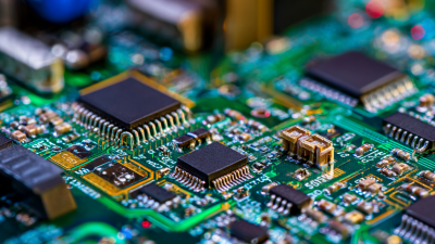
PCB Material Usage in Manufacturing
This bar chart illustrates the percentage of different materials used in PCB manufacturing. FR-4 is the most commonly used material, accounting for 45% of total usage, while the others like CEM-1, CEM-3, Polyimide, and Metal Core have lesser shares.
Key Components of a PCB: Layers and Materials
When designing a printed circuit board (PCB), understanding its layers and materials is crucial. A typical PCB consists of multiple layers, including the substrate, copper layer, solder mask, and silkscreen. The substrate, usually made from materials like FR-4, provides the foundational structure for the PCB. This layer determines the board's physical strength and electrical properties. The copper layer is where the circuit paths are etched, allowing for electrical connections between the components.
The solder mask is a protective layer that covers the copper, preventing oxidation and providing a barrier against solder bridging during assembly. Finally, the silkscreen layer adds markings for component placement and identification, facilitating easier assembly and troubleshooting. Selecting the appropriate materials and understanding their properties can enhance performance and longevity.
**Tips:** When choosing materials for your PCB, consider factors like thermal conductivity and dielectric constant to ensure optimal performance. Additionally, always verify the layer stack-up in compliance with your design specifications to avoid manufacturing issues. Regularly reviewing industry standards can help you stay updated with the latest materials that improve durability and efficiency.
What is PCB Make? A Complete Guide to Designing and Manufacturing PCBs - Key Components of a PCB: Layers and Materials
| Component |
Description |
Material Type |
Typical Thickness |
| Substrate |
The base material that provides mechanical support. |
FR-4, Flexible Materials |
0.5 mm - 3 mm |
| Copper Layer |
Conductive layer used for electrical connections. |
Electrolytic Copper |
1 oz, 2 oz, etc. |
| Solder Mask |
Protects copper traces and prevents solder bridges. |
Epoxy-based materials |
20 µm - 30 µm |
| Silkscreen |
Used for marking component labels and logos. |
Screen Printing Ink |
10 µm - 20 µm |
| Finishes |
Protective coatings applied to copper pads. |
HASL, ENIG, OSP |
Varies |
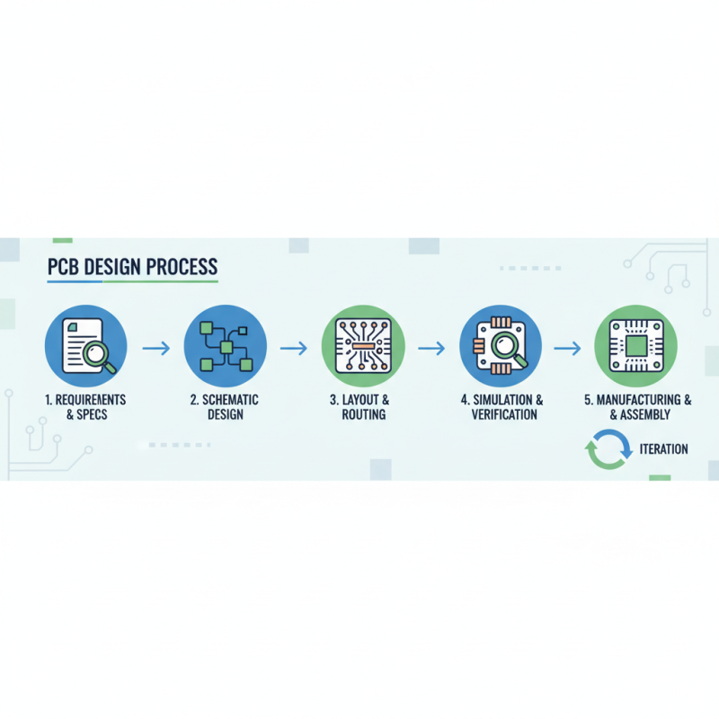
The PCB Design Process: Steps and Best Practices
The PCB design process is crucial for creating effective printed circuit boards that meet the specifications and functional requirements of electronic devices. It typically begins with defining the requirements and specifications, where designers gather all necessary details about the application, functionality, and size constraints. This helps in laying a solid foundation for the design. Once the requirements are set, the schematic design can start, where engineers create visual representations of the circuit’s connections and components.
Tip: Always double-check your schematic for errors before moving on to the layout stage; even minor mistakes can lead to significant issues later in the process.
After completing the schematic, the PCB layout design follows. This step involves placing components and routing electrical connections on the PCB. Attention to detail is vital here, as poor layout can lead to performance issues, such as signal integrity problems or overheating. Utilizing design software can help visualize and optimize the placement, ensuring that all components fit seamlessly and function efficiently.
Tip: Regularly review and validate your PCB layout against the schematic to ensure that all connections are correct and that the design adheres to best practices for PCB manufacturing.
Manufacturing Techniques: From Prototyping to Production
Manufacturing techniques in PCB (Printed Circuit Board) production play a crucial role in transitioning from initial prototypes to full-scale production. In the prototyping phase, methods such as additive manufacturing and etching are frequently employed. Additive techniques allow for rapid iterations and testing of designs, enabling designers to evaluate various layouts without committing to costly production processes. On the other hand, traditional etching involves creating circuit patterns by removing unwanted copper from a board, a method that is well-established and reliable for small batches.
As production ramps up, manufacturers often shift to more scalable methods such as screen printing and surface mount technology (SMT). Screen printing is used for applying solder paste onto boards, ensuring precise placement of components. SMT, which allows components to be mounted directly onto the surface of the PCB, increases component density and reduces overall costs, making it ideal for high-volume manufacturing. Overall, selecting the appropriate technique is essential for achieving efficiency, quality, and reliability in PCB manufacturing, ensuring that designs meet their intended functionalities while remaining cost-effective.
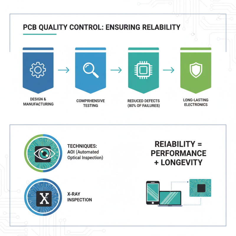
Quality Control and Testing: Ensuring PCB Reliability
Quality control and testing are critical elements in the design and manufacturing process of printed circuit boards (PCBs). The reliability of PCBs directly impacts the performance and longevity of electronic devices. According to a report by IPC (Institute for Printed Circuits), about 80% of PCB failures can be traced back to manufacturing defects, making comprehensive quality control essential. Manufacturers employ various techniques, such as Automated Optical Inspection (AOI) and X-ray inspection, to detect potential defects at different stages of production. These technologies help ensure that even microscopic issues, such as solder joint quality and misalignment of components, are addressed before the PCB reaches the market.
In addition to detection methods, rigorous testing processes contribute significantly to ensuring PCB reliability. This includes Electrical Tests (e.g., In-Circuit Testing and Functional Testing), which evaluate the performance of the PCB by ensuring that it meets design specifications under operational conditions. The International Electrotechnical Commission (IEC) outlines standards for testing PCBs, with some reporting that adherence to these standards can reduce failure rates by as much as 20%. As demand for more sophisticated electronics continues to grow, the implementation of advanced testing techniques becomes vital in maintaining high-quality standards in the PCB industry, ultimately resulting in more dependable electronic devices for end-users.