
Blog
What Is an FPGA Integrated Circuit and How Does It Work?
A Fpga Integrated Circuit is a programmable chip that can change its digital hardware after manufacturing. Unlike a fixed-function processor, it contains configurable logic blocks, routing resources, memory, and input/output connections. Engineers use hardware description languages, such as VHDL or Verilog, to define how these resources should operate.
The design becomes a configuration bitstream. After programming, that bitstream controls lookup tables, flip-flops, multiplexers, and internal wiring. A signal may enter through an I/O pin, pass through several logic blocks, and reach an output within a carefully measured clock cycle. Small embedded memories and digital signal-processing blocks can handle data beside the main logic. It feels flexible. Yet flexibility introduces responsibility.
A practical explanation must include timing, power, and verification. A design can produce correct results in simulation but fail at a specific temperature or clock frequency. Engineers therefore compare simulation results with oscilloscope traces, timing reports, and the manufacturer’s datasheet. They also check setup time, hold time, signal integrity, and configuration reliability during power-up. These details separate a working prototype from dependable equipment.
The concept is powerful, but not effortless. Poorly planned routing may create delays, while excessive parallel logic can increase power consumption. FPGA tools also make recommendations that require human judgment. The exact architecture differs between vendors, so broad descriptions can become incomplete. Understanding those limits makes the Fpga Integrated Circuit easier to evaluate, design, and use in communications, industrial control, imaging, and embedded computing.
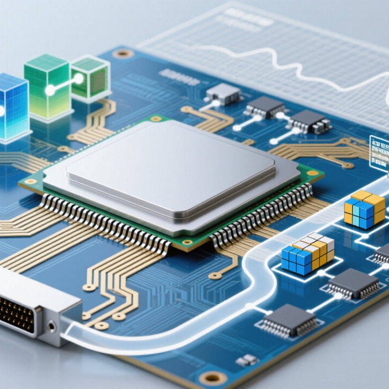
FPGA Integrated Circuits: Definition and Core Purpose
An FPGA integrated circuit is a reconfigurable semiconductor device built from programmable logic blocks, routing channels, memory, and input-output resources. Unlike a fixed-function chip, it can be configured after manufacturing to perform specific digital tasks. Engineers load a hardware description, then the device maps logic functions onto its internal fabric. The result is parallel processing rather than a simple instruction-by-instruction sequence. That difference matters in imaging, industrial control, communications, and edge computing.
Its core purpose is adaptable hardware acceleration. A designer can connect arithmetic units, memory blocks, and signal-processing paths for a particular workload. The configuration remains changeable when requirements evolve. According to the WSTS Spring 2024 forecast, global semiconductor sales were expected to reach 588.4 billion dollars in 2024, rising 13.1% year over year. This expanding market increases pressure for flexible development, especially when product cycles become shorter. FPGA devices can reduce redesign risk, although they usually consume more power and silicon area than highly optimized fixed circuits.
The trade-off is easy to underestimate. Engineers must manage routing delays, clock domains, thermal limits, and timing closure. A design may work in simulation, yet fail under real temperature or voltage conditions. Practical validation needs hardware tests, measured waveforms, and repeated fault analysis. It is not magic. The architecture offers freedom, but freedom can create inefficient logic. According to the 2024 International Technology Roadmap for Semiconductors, advanced systems increasingly depend on heterogeneous computing and specialized hardware. FPGAs fit this direction, but their value depends on disciplined architecture and honest performance measurement.
What Is an FPGA Integrated Circuit and How Does It Work?
FPGA Integrated Circuits: Definition and Core Purpose
An FPGA is a programmable integrated circuit built from configurable logic blocks, lookup tables (LUTs), registers, routing resources, and input/output interfaces. A LUT implements combinational logic by storing one output value for every possible input combination. For a LUT with k inputs, the number of stored truth-table entries is 2k.
LUT Truth-Table Capacity by Number of Inputs
Key Components Inside an FPGA
An FPGA is an integrated circuit built from configurable hardware blocks. Its internal structure can be reshaped after manufacturing. Unlike fixed logic, it lets engineers create specialized digital circuits for control, processing, or signal analysis.
The configurable logic block is a central component. It usually contains lookup tables, flip-flops, and control logic. A lookup table stores output patterns for selected input combinations. A flip-flop holds one bit during a clock cycle. That pairing creates both decision-making and memory.
Small but essential.
The routing fabric connects these blocks through programmable switches. During board testing, I have seen poor routing create unexpected delays, even when the logic seems correct. Long routes can weaken timing performance.
Input/output blocks connect internal signals to external pins. They manage voltage levels, timing, and data direction.
Configuration memory stores the circuit design that controls these resources. At startup, the FPGA loads this configuration from an external or internal source. Clock-management circuits distribute stable clock signals across the device.
Dedicated memory blocks support buffers, tables, and temporary data storage. Many devices also include arithmetic units for multiplication and accumulation. These components reduce the need to build every function from basic logic.
Still, the neat block diagram can be misleading. Real performance depends on placement, routing, clock design, and power conditions. One timing problem may come from an overlooked connection rather than faulty logic. Hardware rewards careful measurement.
How FPGA Logic Is Configured and Programmed
An FPGA is an integrated circuit filled with configurable logic blocks, routing channels, and memory elements. Its behavior is not fixed during manufacturing. Engineers load a configuration bitstream that defines how these resources connect and operate.
The design usually begins in a hardware description language. Tools translate that code into lookup-table contents, registers, wiring paths, and timing constraints. A programmer then transfers the bitstream through a development interface or embedded controller. After power-up, the device reads the configuration from non-volatile storage and rebuilds its logic. Timing still bites. A circuit may produce correct results but fail at high frequency because signals arrive too late.
According to the 2024 FPGA Market report from MarketsandMarkets, the global FPGA market is projected to grow from about 10 billion dollars in 2024 to more than 17 billion dollars by 2029. This demand reflects flexible acceleration in communications, industrial control, aerospace, and edge computing. The Semiconductor Industry Association reported that global semiconductor sales reached 526.8 billion dollars in 2023, showing the scale of the ecosystem supporting programmable hardware. In practice, engineers repeatedly simulate, synthesize, inspect timing reports, and test the physical board. My own caution is simple: successful compilation proves little. Power noise, clock placement, and overlooked reset behavior can still expose weaknesses.
Step-by-Step Operation of an FPGA Circuit
An FPGA integrated circuit is a programmable hardware device built from configurable logic blocks, routing channels, memory elements, and input/output connections. Unlike a fixed-function circuit, it can be reshaped after manufacturing. Its operation begins with a hardware design created in a specialized development environment. The design is converted into a configuration file, often called a bitstream.
When power is applied, the FPGA loads this bitstream into configuration memory. The stored settings control tiny switches, lookup tables, registers, and signal routes inside the chip. Input signals then enter through configured pins. A lookup table processes Boolean logic, while flip-flops hold values on clock edges. The result moves through selected routing paths and leaves through output circuitry.
Timing matters at every step. A clock may coordinate thousands of operations, but signals still need enough time to travel between logic blocks. In practical testing, a design can pass simulation yet fail on a physical board because of delay, noise, or an overlooked clock constraint. That weakness is instructive. Engineers measure waveforms, inspect resource usage, and revise the design repeatedly. Some functions may run in parallel, which gives an FPGA strong performance for specialized tasks. However, parallel hardware can consume more power and logic resources than expected. Careful verification remains essential before trusting the circuit in equipment.
Common Applications and Design Considerations
An FPGA integrated circuit contains configurable logic blocks, flip-flops, memory, and programmable routing. Engineers define its hardware behavior after manufacturing. The device can process several operations in parallel, unlike a conventional processor that follows a mostly sequential program. This structure supports real-time control, image processing, communications equipment, robotics, and scientific instruments. A motor controller, for example, may read sensors, calculate position, and generate protective signals within microseconds.
Application needs should guide the design. Developers must examine timing, power consumption, thermal limits, input-output voltage, and available internal resources. A design may simulate correctly but still fail when signals arrive with unexpected delays. Clock-domain crossings require careful synchronization. Safety-related systems also need fault detection, independent checks, and documented verification. More logic is not always better. Extra features can increase routing congestion and make testing harder. That tradeoff is easy to underestimate.
Tips: Define timing requirements before writing hardware logic. Reserve memory and processing resources early. Measure power under realistic workloads, not idle conditions. Use small test modules before integrating the complete system. Keep revision records. They reveal hidden assumptions. A practical review should question whether an FPGA is truly necessary; a simpler circuit may reduce cost, heat, and maintenance. Still, flexibility can justify the added complexity when requirements may change.
What Is an FPGA Integrated Circuit and How Does It Work? - Common Applications and Design Considerations
| Category | FPGA Element or Concept | Typical Characteristics | How It Works or Why It Matters | Common Design Considerations |
|---|---|---|---|---|
| Core Architecture | Programmable logic fabric | A two-dimensional array of configurable logic blocks connected by programmable routing | The device is configured after manufacturing to implement digital circuits such as processors, controllers, filters, and communication interfaces. | Balance flexibility, logic utilization, timing performance, routing congestion, and power consumption. |
| Logic Resources | Look-up tables (LUTs) | Common FPGA LUTs implement Boolean functions with approximately 4–6 inputs | Configuration memory determines the LUT output for every possible input combination, allowing many combinational functions to be created. | Large or deeply nested logic may require multiple LUTs and additional routing, increasing delay and resource usage. |
| Sequential Logic | Flip-flops and registers | Usually available alongside LUTs in configurable logic blocks | Registers store one bit of state and synchronize operations on clock edges, enabling pipelines, counters, finite-state machines, and data buffers. | Meet setup and hold requirements, limit excessive fan-out, and place pipeline registers where timing paths are long. |
| Interconnection | Programmable routing network | Switch matrices and wire segments connect logic blocks, memory, DSP units, and input/output resources | Routing resources determine how signals travel through the device after synthesis and place-and-route. | Routing congestion can reduce maximum clock frequency even when sufficient logic resources remain. |
| Memory | Embedded block RAM | Synchronous dual-port or single-port memory blocks; capacity varies widely by device family | Stores coefficients, instructions, lookup tables, packets, image lines, and intermediate results close to the processing logic. | Choose memory width, depth, port mode, initialization method, and read latency carefully. |
| Arithmetic Processing | Dedicated DSP or arithmetic blocks | Hardware multipliers, adders, accumulators, and pipeline registers | Accelerates multiply-accumulate operations used in digital filters, motor control, image processing, and machine-learning workloads. | Use appropriate operand widths and fixed-point formats to prevent overflow while conserving resources. |
| Clocking | Clock-management and distribution resources | Dedicated low-skew clock networks with frequency multiplication, division, and phase adjustment capabilities | Provides stable, synchronized timing for different logic regions and interface protocols. | Minimize clock-domain crossings, use synchronized control signals, and verify clock constraints. |
| Input and Output | Configurable I/O banks | Support for multiple voltage levels, signaling standards, input thresholds, and output drive strengths | Connects internal logic to sensors, converters, memories, processors, displays, and communication links. | Check voltage compatibility, pin assignments, signal integrity, termination, and interface timing. |
| Configuration | Configuration memory and bitstream | A bitstream defines LUT contents, routing connections, register settings, and I/O behavior | The bitstream is loaded during power-up or through an external configuration process; many SRAM-based devices must be reconfigured after power is removed. | Consider boot time, configuration security, field updates, fallback images, and nonvolatile storage. |
| Design Flow | HDL, synthesis, placement, and routing | Common hardware description languages include VHDL and Verilog/SystemVerilog | Design tools convert behavioral or structural descriptions into a technology-mapped circuit and then assign physical resources. | Use constraints for clocks, I/O timing, false paths, and physical locations; verify both function and timing. |
| Performance | Parallel and pipelined processing | Multiple operations can execute concurrently; practical clock rates depend on architecture and device implementation | Parallel datapaths provide high throughput and predictable latency for streaming workloads. | Optimize critical paths, pipeline long calculations, and distinguish throughput from single-operation latency. |
| Power | Dynamic and static power | Power depends on voltage, clock frequency, switching activity, temperature, routing, and utilized resources | Every signal transition consumes dynamic energy, while leakage and bias currents contribute to static power. | Reduce unnecessary switching, gate or disable unused logic, select suitable operating frequencies, and provide adequate thermal management. |
| Common Application | Digital signal and image processing | Filtering, Fourier transforms, video pipelines, feature extraction, and data conversion support | Parallel arithmetic and streaming architectures process large data volumes with deterministic timing. | Manage sample rates, data widths, buffering, memory bandwidth, and end-to-end latency. |
| Common Application | Industrial control and robotics | Motor control, sensor aggregation, pulse generation, safety monitoring, and real-time feedback | Hardware logic can respond to multiple inputs simultaneously with predictable response times. | Address deterministic behavior, fault handling, isolation, certification requirements, and safe startup states. |
| Common Application | Communications and networking | Packet processing, protocol bridging, modulation, error correction, and high-speed interface control | Custom datapaths can handle several protocol stages in parallel and adapt to evolving standards. | Verify protocol compliance, buffering, line-rate throughput, clock-domain crossings, and signal integrity. |
| Advantages | Reconfigurability and hardware parallelism | Function can be updated without redesigning the silicon; many operations run concurrently | Shortens development cycles and supports product variants, prototypes, and field upgrades. | Account for engineering effort, tool complexity, configuration management, and hardware verification. |
| Limitations | Resource, power, and timing constraints | Routing overhead and programmable interconnect may consume more area and power than a fixed-function circuit | The best architecture depends on workload, production volume, latency, power budget, and required flexibility. | Evaluate total development cost, unit cost, thermal design, verification complexity, and long-term availability. |
