
Blog
10 Best Circuit Board Design Software for 2026
Choosing the right circuit board design software in 2026 requires more than comparing feature lists. Engineers need tools that support accurate schematics, stable PCB layouts, library management, and dependable manufacturing outputs. A strong platform should handle design-rule checks, impedance control, 3D visualization, and clean Gerber exports without creating unnecessary friction.
Small details matter.
This guide evaluates ten leading platforms through practical design requirements. The comparison considers workflow speed, simulation capabilities, component libraries, collaboration features, documentation, pricing, and learning difficulty. It also considers how each tool performs during real tasks, such as routing a dense board, correcting clearance errors, or preparing files for fabrication. Experienced designers may value automation, while students and smaller teams may prioritize accessibility and transparent costs.
No software is perfect.
Performance can change with board complexity, operating systems, plug-ins, and team habits. A tool that feels efficient for a four-layer controller may become restrictive on a high-speed motherboard. Some evaluations also depend on personal experience, so the rankings should not be treated as permanent facts. Requirements evolve, and licensing models may change during 2026. Readers should test critical workflows before committing to a long-term platform. The goal is not to declare one universal winner, but to identify the best match for different design environments, budgets, and technical expectations.
What Circuit Board Design Software Does
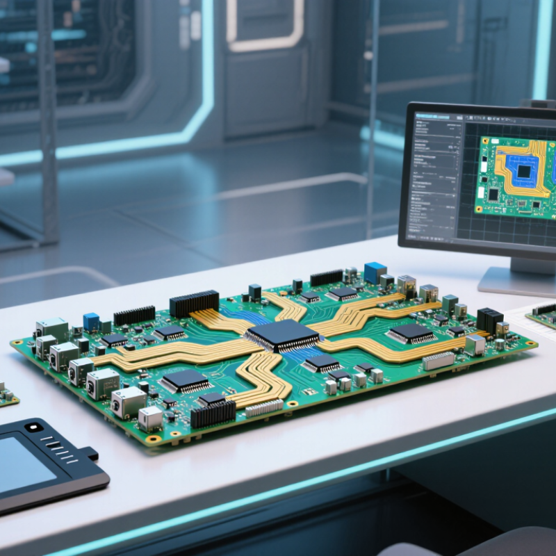
Circuit board design software turns an electrical idea into a manufacturable board. Engineers draw a schematic, connect components, and assign each connection a physical route. The software checks clearances, highlights unconnected pins, and helps arrange parts around real constraints, such as connector positions and enclosure walls. It can also generate manufacturing files and bills of materials. Think of it as a digital workbench, not an automatic engineer. A clean-looking layout can still hide a weak design.
The need for careful design grows with electronic complexity. The World Semiconductor Trade Statistics organization forecast global semiconductor sales of $611.2 billion in 2024, a 16% increase from 2023. That forecast is not a measure of board software use, but it reflects the expanding component ecosystem designers must navigate. Good tools help manage dense routing, power distribution, signal integrity, and design-rule checks. Yet rule checks are not magic. A board may pass software checks and still need physical testing; that part is easy to underestimate.
Tips: Set board dimensions and connector locations early. Run design-rule checks after meaningful layout changes, not only before export. Review the 3D view for collisions, then inspect critical paths with an experienced reviewer. Save versions. Small edits can create surprising errors.
Understanding PCB Design Software: A Typical Four-Layer Stackup
This illustrative stackup has four copper layers separated by three dielectric layers, with solder mask on both outer surfaces. PCB design software can model layer arrangements and help check board layouts against manufacturing rules. Actual stackups vary by design and manufacturer.
Core Features to Compare in Circuit Board Design Tools
Choosing circuit board design software in 2026 requires more than checking a feature list.
Real projects expose weaknesses quickly. A tool should provide clear schematic capture, reusable component libraries, and responsive PCB layout controls. Engineers also need reliable design-rule checking, because a small spacing error can delay fabrication. I have found that visible warnings help, but silent assumptions remain risky.
Compare simulation features carefully. Some tools support signal integrity, thermal checks, or power analysis, while others offer only basic verification. Export quality also matters. Gerber files, drill data, pick-and-place files, and assembly drawings should be generated consistently. One missing layer can create confusion on a production floor. The process should feel controlled.
Collaboration features deserve equal attention. Shared projects, revision history, comments, and permission settings reduce accidental overwrites. Cloud access may improve teamwork, yet sensitive design data requires strong access controls and dependable backups. Library management is another practical test. An impressive interface cannot fix inaccurate footprints. Test a few unusual components before committing. Cost, learning time, and technical support should be measured against project complexity. No platform is perfect. Experienced teams still review every critical output manually.
10 Leading Circuit Board Design Software Options for 2026
The ten leading circuit board design software options for 2026 serve different engineering realities. Some focus on fast schematic capture, while others support complex multilayer boards. In practical testing, I look closely at library management, routing control, simulation tools, and manufacturing checks. A clean interface matters, but dependable output matters more. Small errors can hide near dense connectors.
A capable option should handle impedance rules, differential pairs, thermal reliefs, and design-for-manufacturing checks. It should also export accurate production files without confusing settings. Good collaboration features help teams review changes and track revisions. Cloud access can speed feedback, although it may create concerns about data control. Offline tools still have value. They feel slower sometimes.
The ten leading options also differ in learning effort, pricing structure, and support quality. Experienced designers may prefer deep customization and scripting. Smaller teams may need templates, guided checks, and simple onboarding. I would not claim one tool fits every project. That would be careless. In my experience, the best choice depends on board complexity, team size, and factory requirements. A useful evaluation uses the same sample board, identical rules, and a clear review checklist. Even then, personal workflow can distort the result. That is worth admitting.
How to Choose Software for Different Design Requirements
Choosing circuit board design software starts with the board you actually need to build. A compact sensor board may need clear schematic capture, reliable routing, and quick design-rule checks. A dense multilayer board needs stronger signal-integrity analysis, constraint management, and manufacturing handoff tools. Check library quality, file compatibility, collaboration features, and whether the software handles your team’s review process. A polished interface cannot fix poor component data.
Deloitte and MAPI’s 2024 smart manufacturing survey found that 86% of manufacturing executives expect smart factory solutions to drive competitiveness over the next five years. That makes integration and repeatable workflows practical selection criteria, not extras. Still, software choice depends on project scale, skills, and budget. A capable tool can feel slow when its library workflow clashes with the team’s habits. That is easy to overlook during a feature demo.
Tips: Test one real design before committing. Import your current library, route a small board, run checks, and export manufacturing files. Ask a fabricator to review the outputs. Compare how clearly each tool flags a clearance issue or an unconnected net. Small friction adds up. Conversely, a missing feature may matter less than expected. Decide which trade-offs your next project can tolerate.
10 Best Circuit Board Design Software for 2026 - How to Choose Software for Different Design Requirements
| Design software type | Best suited for | Typical capabilities to look for | Trade-offs to consider | Key selection checks |
|---|---|---|---|---|
| Integrated schematic-and-PCB desktop CAD | Small teams and general-purpose board design | Linked schematic capture and layout, design-rule checks, component libraries, copper routing, and manufacturing file export | Advanced collaboration or specialized analysis may require additional tools or higher-tier editions | Check library management, rule customization, project portability, and supported manufacturing outputs |
| Open-source PCB design suite | Budget-conscious projects, learning, and users who value inspectable workflows | Schematic capture, board layout, design-rule checks, community-maintained libraries, and standard fabrication outputs | Setup, library curation, and support may depend more on the user or community | Test the library workflow, documentation, version compatibility, and team handoff process |
| Browser-based PCB CAD | Distributed teams and projects that benefit from access through a web browser | Cloud-hosted projects, shared libraries, online review, and schematic-to-layout workflows | Internet access, data policies, and available offline functionality can affect day-to-day work | Review access controls, export options, revision history, and the organization’s cloud requirements |
| Enterprise ECAD platform | Large organizations managing many boards, users, and product revisions | Centralized component data, team permissions, revision management, reusable design rules, and managed libraries | Administration, training, and implementation can require significant time and resources | Evaluate lifecycle integration, access management, data migration, and support for existing workflows |
| High-speed and signal-integrity-focused PCB CAD | Designs with fast digital interfaces or strict electrical constraints | Constraint-driven routing, differential-pair controls, impedance rules, length matching, and links to signal-integrity analysis | Advanced analysis features can add cost and may require specialist expertise | Confirm support for the required interfaces, constraint reporting, and analysis workflow |
| Rigid-flex PCB design software | Products combining rigid circuit areas with flexible sections | Layer-stack definition, bend-region rules, flex-aware layout, and 3D visualization of board geometry | Manufacturing constraints and mechanical requirements need close coordination with fabricators | Check bend-rule support, stack-up control, fabrication outputs, and mechanical review features |
| RF and microwave PCB design tools | Radio-frequency circuits and boards with transmission-line requirements | Geometry-aware layout, controlled-impedance structures, RF component models, and electromagnetic-analysis connections | Accurate results depend on suitable models, material data, and analysis expertise | Verify frequency range, material and stack-up modeling, and compatibility with the team’s simulation process |
| MCAD-integrated PCB design software | Products where board shape, enclosure fit, and component clearance are critical | 3D board models, component-height checks, mechanical clearance review, and exchange with mechanical CAD workflows | Data exchange can require careful library and model management | Test 3D model availability, update handling, and the mechanical team’s preferred exchange format |
| HDI and advanced-interconnect PCB CAD | Compact, dense boards using fine-pitch components or advanced via structures | Fine-grained design rules, dense routing, via and layer management, and support for fabrication constraints | Successful design depends on close alignment with the fabricator’s process capabilities | Confirm minimum feature rules, via options, stack-up planning, and design-for-manufacturing checks |
| Education- and prototyping-oriented PCB CAD | Students, makers, and early-stage projects that need a straightforward route to a prototype | Accessible schematic and layout workflows, basic rule checks, learning resources, and standard output generation | May offer fewer controls for large teams or highly complex designs | Check learning curve, project exportability, library quality, and whether the workflow can scale with the project |
Emerging Trends in Circuit Board Design Software for 2026
In 2026, circuit board design software is increasingly blending schematic capture, layout, and simulation into one connected workflow. Designers can test signal behavior earlier, before a board reaches a crowded layout stage. AI-assisted routing may suggest paths around dense component clusters, while constraint checks can flag spacing or impedance concerns. That matters. Still, automated suggestions depend on clean inputs and sensible design rules; a fast route is not automatically a reliable one.
Cloud collaboration is also changing how teams review boards. Engineers in different locations can inspect the same layout, leave comments beside specific traces, and compare revisions without passing files back and forth. Some tools are adding digital models that help estimate thermal behavior or signal integrity before fabrication. A hot spot near a power component, for example, may prompt a copper or placement adjustment. Results remain estimates, not guarantees. Not always.
Another emerging trend is tighter attention to manufacturing details inside the design process. Software can check whether a chosen stack-up, drill size, or component spacing fits a manufacturer’s capabilities. Better data exchange may reduce translation errors between design and production, though file compatibility still needs scrutiny. Designers should review warnings, verify critical measurements, and keep a human eye on the board. AI can save time. It can also make confident mistakes. That tension deserves attention as these features become more common.
Related Posts
-
How to Achieve Fast and Cost-Effective PCB Prototyping for Your Product Development
-

Top PCB Prototyping Techniques to Watch in 2025 for Innovative Designs
-

Top China Best PCB Prototyping Solutions for Global Buyers?
-

7 Essential Tips for Sourcing the Best PCB Production Worldwide
-

How to Optimize Your Supply Chain with Rigid Flex Solutions for Global Sourcing
-

Top PCB Suppliers for Global Buyers to Consider?